
PCB design is the procedure of placing the circuit like a physical printed circuit board. The way you design the Printed Circuit Board is essential as it determines whether your PCB will turn out to be a success or failure. If you have designed it in an improper way, it might result in a low functioning and inconsistent printed circuit board.
However, many novices are wondering about how to properly design a printed circuit board. If you are also interested in the same question, we are here to help you out. Here, we will talk about the best tips that will make it easy for you to design a PCB properly.
Table of Contents
Top 9 Tips Explaining How To Design A Printed Circuit Board
Some companies offer custom printed circuit board designs and PCB layouts for already created design schematics. If you want to enhance and optimize the PCB design, make sure to click here, which provides services at a reasonable price. Below we will talk about the best tips which will help you design an excellent Printed Circuit Board.
1. Avoid Using The Autorouter For Everything
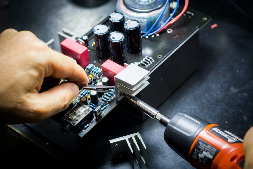
source: unsplash.com
Several printed circuit board design software maintains an autoroute element that will automatically do the routing. However, it is better not to autoroute everything. You can use autorouting in some situations, for example, to check whether all the components are placed correctly.
You can also use autorouting for recognizing the blockages and various other crucial connection points. When you are stuck at something or do not have any idea of how to start routing, it is better to use autorouting as a reference source. It is best to avoid using autorouting because it is not precise sometimes and often ignores symmetry. Hence, only use the autorouting for the mentioned situations.
2. Make Vital Nodes Available
Make sure to keep the critical nodes easily accessible. For example, if your PCB is not functioning appropriately, you might need to check the inside signals. Hence, before creating the PCB, you have to think about which nodes will be vital to solve the circuit problems and make them available.
However, if you can not reach them easily, it is better to add a test point that is attached to them. There are several aspects of test points, but the test points that set a loop are excellent for test investigations with pins.
3. Make Sure To Leave Some Gap Between Components
source: unsplash.com
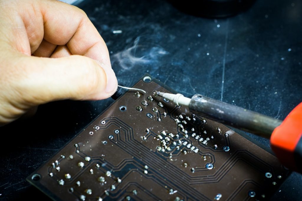
Many of you might be designing the printed circuit board by keeping the components as close as possible. However, doing that will leave no space for the routing of cables. It will be much better for you to keep enough room between components so wires can scatter. If the parts possess additional pins, it will require more open space. Leaving some gaps will make the soldering simple.
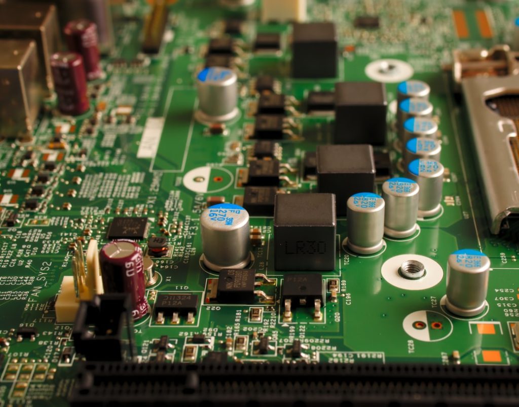
4. Keep Sufficient Trace Width
source: unsplash.com
It is crucial to keep in mind that traces retain electrical resistance. Due to that, when current passes through them, there will be a drop in the voltage, power dissipates, and heat will produce. So, you have to make sure to prevent surplus heat in the circuit. By improving the width of the traces, it is possible to decrease the amount of heat accumulation.
5. Placing Components
You need to place the components properly to make a functional circuit. Some specific components should not be put close to each other. For instance, you need to put the heat-sensitive electrolytic capacitors far away from particular parts, such as heat-generating diodes, resistors, and inductors.
Make sure to keep the component in the same orientation. For that, almost all parts come with a typical pin numbering, so it will be easy for you to put them in place. Before putting any components to design the PCB, consider their functions and connection with each other.
6. Print The Format To Check If Components’ Sizes Fit
After placing each and every component or if components are already acquired, it is best to print out the structure. If you want, you can put each part on the printed layout paper to analyze whether the components can fit into their place. However, keep in mind that sometimes datasheets might contain mistakes.
7. Utilize 45° Trace Angles
source: unsplash.com
Traces operate through the entire printed circuit board and near the components. You might think it will be effective to develop 90° angles at intersections and corners, but it is not a good idea. It is because there is a high likelihood the external corner of a 90° trace might cut thinner than it has to be. Besides that, sharp right-angle bends are hard to maintain uniform trace width.
It is better to use 45°, which is the sweet spot. The 45° trance angles will make it simple to intertwine between pads and still generate a stunning design. In addition to that, it is much easier to inscribe.
8. Establish A Ground Plane
source: unsplash.com
The common ground is essential because it acts as a reference point for the traces to calculate the voltage. Though you can use traces to route to the ground, it might result in several connections on the PCB. It happens due to the fluctuating resistance values of the traces, which leads to various voltage drops. You need to create a specific ground plane in the PCB design to deter establishing multiple ground connections.
9. Use The Silk Layer
The silk layer is often standard in proficient PCB manufacturers, which is relatively beneficial for labeling. It is used in several routing software applications as well. With the help of this layer, it will be easy to label the components. In addition to that, you can incorporate essential information, such as board type, revision number, manufacturer, and many more.
Bottom Line
By following the above-mentioned tips you can easily create a printed circuit board design successfully. Keep in mind that planning ahead will lessen the PCB expenses. As formulating the PCB is significant, be cautious and take your time to design the layout.