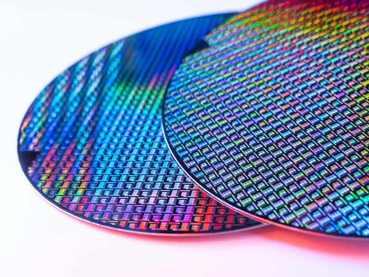
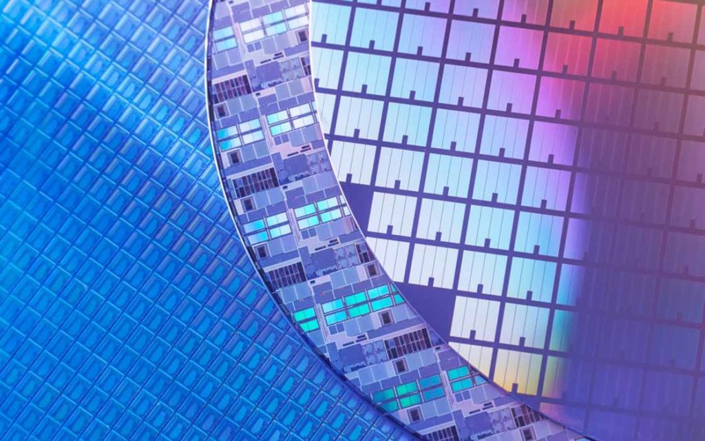
A patterned wafer is a small balanced, disc-like stuff, which generally comprises silicon or some other semiconductor substance and gets covered with a tiny coating of a substance like a nitride or an oxide. You can produce solar panels based on silicon and Microelectronic circuits (integrated circuit ICs) from these wafers. It works as the underlayer in those structures. Patterned Silicon Wafers are commonly employed in nearly every aspect of humankind and technological development. For instance, they can be utilized in an extensive scope of industries, from wearable technology to geothermal power. Because of their strength above all other microprocessor substances, patterned wafers are the utmost broadly operated resource in the technological sector. Besides providing a better option contrary to other metallic materials, they are even extensively accessible all over the globe. You can analyze the diverse uses in detail below.
Source: thomasnet.com
Table of Contents
Different Uses Of Patterned Wafers In The Modern World
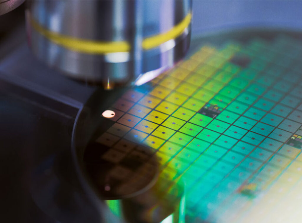
As you know, patterned wafers are mainly used in Microelectronic circuits since it comprises the necessary elements of ICs. Integrated circuits are a group of Electrical segments & circuitry that collaborate to accomplish an exact piece of work. Patterned wafers have been confirmed to be a better long-lasting choice, although various microprocessors have been examined over the years. You can use these wafers in a considerable diversity of devices. Keep reading to understand what exactly are the uses of patterned wafers.
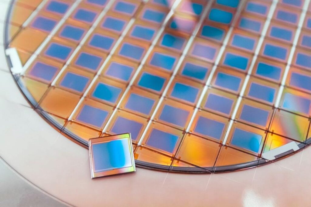
Patterned Wafers In Solar Panels
To capture better sunrays and improved effectiveness, solar panels require patterned wafers. You can generally operate resources such as microcrystalline or nanocrystalline silicon, single-crystal silicon, and tellurium cadmium. Creating methods such as the Float Zone (FZ) process increases solar panel capability by almost 25 percent. Solar panels adhere to equivalent manufacturing processes likely to microprocessors. The sterility and grade levels required for solar panels may not be as challenging as those used for electronics and other computing.
Source: cdiglobal.com
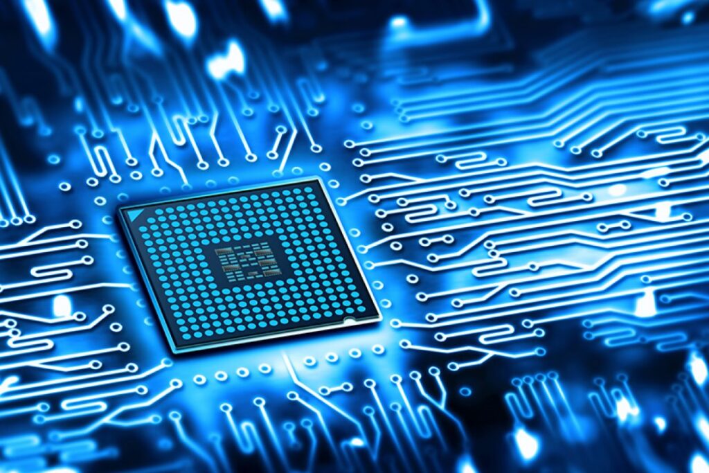
Semiconductors Industry
Microprocessors are the elementary units for many voltaic gadgets and appear in diverse formations and figures involving capacitors, junction rectifiers, and ICs. You may manufacture it utilizing silicon chips, as it extends their density and capability. Semiconductor units are used in photo-sensors, electrical appliances, and even laser shafts because they can manage a comprehensive array of electromotive force or energy.
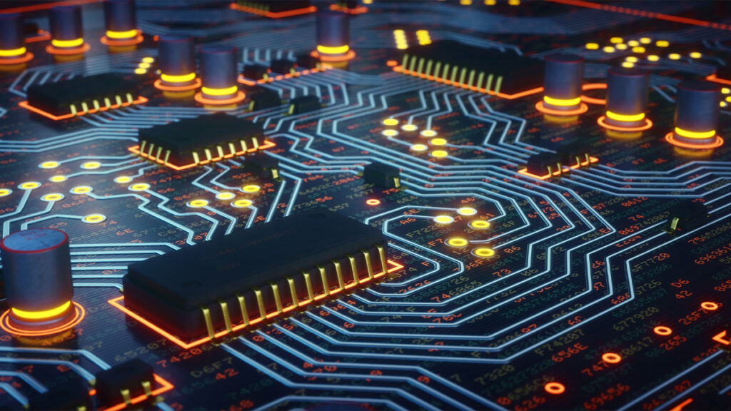
Patterned Wafers In Computing And Electronics
Patterned wafers are proven effective in expanding the information age because it gets broadly employed in the computing and electronics sectors. Pattern silicons create DEE-RAM chips, a kind of (ICs) Integrated Circuit. It drives these silicons to detail deeply in the information technology sector. Furthermore, Patterned wafers can help you to fabricate many gadgets like digital phones, digital home devices, motorcar electronics, and unmanned aerial vehicle technology. Almost every electronic chip gadget has a top-level usage possibility for patterned silicons. Recent forming approaches and impulsive techniques push them to be better functional and well-organized.
Silicon Wafers In Medical Equipment
Do you know silicon wafers even get used in the medical instrument industry? They get utilized to make detectors and different elements in medicinal gadgets like cardiac pacing devices, defibrillators, and glucose visual display units. These instruments demand top levels of accuracy and dependability, and silicon wafers play a crucial part in their manufacturing.
Source: market-prospects.com
Patterned Wafers Used In Optics
Usually, polished patterned wafers get uniquely fabricated for optics grading. These silicons are the ideal efficient resources with employment in Contemplative optics and Heat radiation. To make Patterned silicons for optics Float Zone (FZ) Process or Czochralski (CZ) silicon techniques of manufacturing get operated. It is because both procedures hardly deliver any faults and are farther up than all other processes. You may find its usage in micro-optic and optical fiber gadgets globally. The (CIS) Contact Image Sensors created with (CMOS) Complementary Metal-Oxide-Semiconductor transistors employed in camcorders can be its precise illustration.
Used In Sensors
Silicon-patterned wafers can get used to produce the detecting features in sensors. They identify modifications in climate, pressure, or different observables. These sensors get often employed in an extensive array of industries.
Micro Fabricated Fluidics
Now you may use Patterned silicons to create instruments for sharply handling and manipulating fluids at the nano-scale. Also, you can make nanoscopic designs and microchannels viable by shaping a wafer’s texture. They may get employed for diverse utilizations involving microfluidic instruments, near-patient testing, and pharmaceutical compound delivery methods.
Silicon Wafers In Wearable Techs
You might fabricate extendable and adjustable capacitors for wearable gadgets with the help of silicon wafers. Detectors and circuits that can adjust according to the mildew of the human figure can get completed by patterning the wafer surface.
Source: okmetic.com
Silicon Wafers In Aerospace
As you know, these silicons have exceptional features and qualities. They are often used in the aeronautics sector as a crucial resource and get operated for guarding and protecting fragile instruments from intense climates. They have been a decent and reliable option for a long time because of their expansive usage and suffering in extreme climate conditions. Patterned wafers are especially valuable for Original Design Manufacturer (OEM) purposes, also for repairing, maintaining, and renovating. They are a reasonable choice because of being delivered in double tubes and boxes, optimizing efficiency and decreasing wastage.
Used In (MEMS) Micro Electro Mechanical Systems
MEMS are small instruments incorporating mechanized and electrical elements and may get created with silicon wafers. Complicated designs for the purpose of diverse uses, involving detectors, accelerometers, and microfabricated fluidic gadgets, can be constructed only by patterning the wafer surface.
Source: geaerospace.com
Bottom Line
Ever since silicon patterned wafers got operated in the microprocessor industry, they have expanded a lot. When it comes to the evolution of computing, information technologies, and electronics, they play an essential part. Silicon wafers have so much capability in diverse state-of-the-art areas, such as solar panels, microfabricated fluidics, micro-electro-mechanical systems, optics, and wearables. Expenditure, output, and expandability are some of the complexities you may consider. But because of non-stop fabricating and technological advancements, you can expect them to be essential in specifying the fate of electronics, wellness, and energy sources.