Depending on the specifications of the motherboards they have to install in, PCBs come in a wide array of thicknesses. Based on this copper thickness, they are either termed as standard or a heavy copper. Both have their own unique features and properties that make them suitable for different applications. That is why the developers change the copper thickness to meet the needs and requirements of the customers.
This article aims to provide a comparative analysis of standard PCB and heavy copper PCB that will help you understand the basic design and utility of each type.
So, keep reading!
Table of Contents
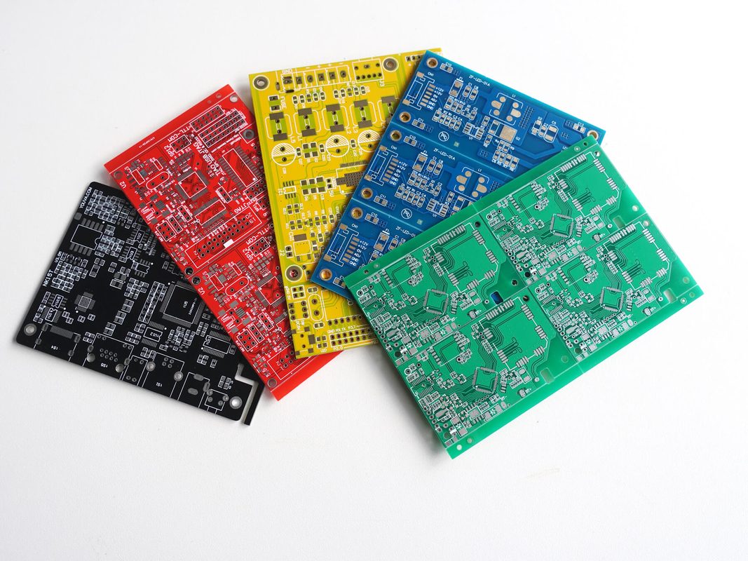
Standard Thickness PCBs
img source: pinimg.com
Standard PCBs, as the name implies, have an internationally recognized thickness. Generally, the thickness of a standard PCB is 1.57mm and it is still the most widely used type – both in domestic and commercial products and equipment. These can easily handle the weight of integrated transistors, circuits, and normal RC components – even when their dimensions exceed 500mm*500mm. Standard thickness PCBs are mostly preferred for low current inputs.
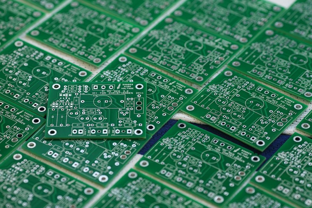
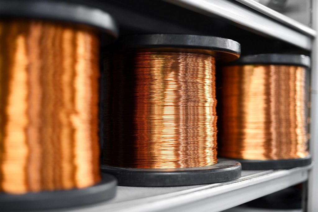
Heavy-Copper PCBs
img source: alicdn.com
These have no established IPC definition other than that their thickness is more than that of standard boards. However, the range of copper thickness of heavy copper boards is supposed to be from 105 to 400 µm. These can easily handle high current outputs and are, therefore, used for heavier duties such as optimization of thermal management. Also, the presence of a thick copper layer allows them to withstand high current loads and dissipate heat easily. Generally, thick layer PCBs are double-layered or multilayered while more information about them can be found here. Because of its high-functioning capabilities, the demand for thick layer PCBs has increased substantially in recent years.
They can withstand high temperature, pressure, tough industrial conditions, and extremely corrosive atmospheric environments and hence used in hot melt welding methods like blowing Oxygen at a high melting point.
Comparing Standard PCBs and Heavy Copper PCBs
img source: fischer.com
Let us compare the characteristics of both:
Thickness
The use of heavy copper PCBs has increased manifold compared to standard. The former has a copper weight of around 4 ounces compared to 1 or 2-ounce of copper in the standard PCBs I.e., 2-4 times heavier. This extra thickness of the copper plate allows heavy copper boards to conduct large current, maintain proper heat dissipation and distribution, and perform multi-functions in a limited space. Other than that, they demonstrate enhanced mechanical strength and carry out complex functions with maximum capacity – with minimum risk of circuit failure.
Manufacturing Process
In terms of the preparation process, the standard PCBs are manufactured through platting and Copper etching methods. On the other hand, differential etching and step platting methods are used by the developers to manufacture heavy copper PCBs.
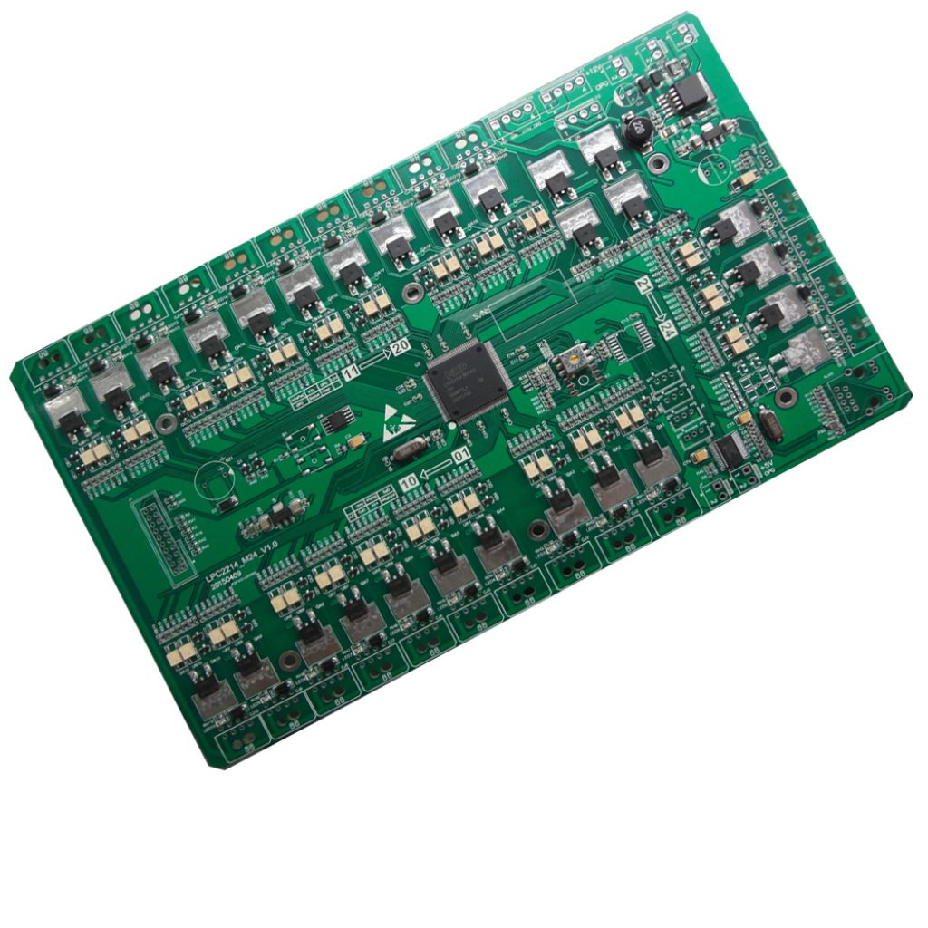
Capabilities

img source: chatlogy.ai
As mentioned earlier, heavy copper boards are designed for performing heavy duties such as those in the telecommunication sector. They not only increase the capacity of end electronic products but also improve the efficiency of the end product. Standard PCBs, on the other hand, are better suited for lighter activities and mostly come in a single layer.
Current Conductivity
Standard units can conduct a lesser amount of current and can become inefficient or damaged if higher amounts of current output are passed through them. Contrarily, heavy copper boards can easily conduct higher amounts of current without the risk of circuit failure or damaging.
Effect on Capability of Board
Heavy Coppers increase the anti-stress capability of the electronic product in which they are used. Conversely, the standard ones do not affect the efficiency or ability of the printed board and rather perform their functions irrespective of the capability of the board.
Mechanical Properties
img source: si-cdn.com
The presence of Copper increases its mechanical strength and capabilities. Since more copper (almost 4 times more than that of standard PCBs) is used in the manufacturing of heavy copper PCBs, they display better mechanical strength. While standard units have less mechanical strength due to the thin layer of copper.
Measurement Unit
The copper quantity in standard boards is measured in ounces (oz). As a standard, 1 oz Copper is used during the manufacturing of a standard PCB – it has a thin layer of copper.
On the other hand, heavy coppers have a higher amount of copper used in them and have, therefore, thicker diameter than the standard PCBs. In most cases, 2 to 4oz copper is used in the manufacturing of a heavy copper board.
Thermal Distribution
The thermal distribution of a heavy copper PCB is efficient and it can better manage thermal distribution to various components and also ensure proper thermal dissipation – and are therefore efficient in working performance. This high thermal efficiency makes heavy copper units an ideal choice for heavy-duty applications where heat generation is higher. Contrarily, the standard is not as efficient in thermal distribution and dissipation as heavy copper PCBs.
The above comparison clearly shows that heavy coppers are better than standard boards in a plethora of ways. More and more companies are manufacturing heavy copper PCBs for the very same reasons. When it comes to sophisticated and smart electronic appliances, heavy copper PCBs are always the first priority of the customers. Moreover, these circuits can also be easily integrated with the standard circuit boards.
It is pertinent to mention that leaps in technology have made it possible for developers to reduce the size of the heavy copper PCBs as they can now be manufactured by the combination of etching and plating – not separately. It helps developers to remove any extra edges and sidewalls of the boards.